PCB DESIGN SERVICE
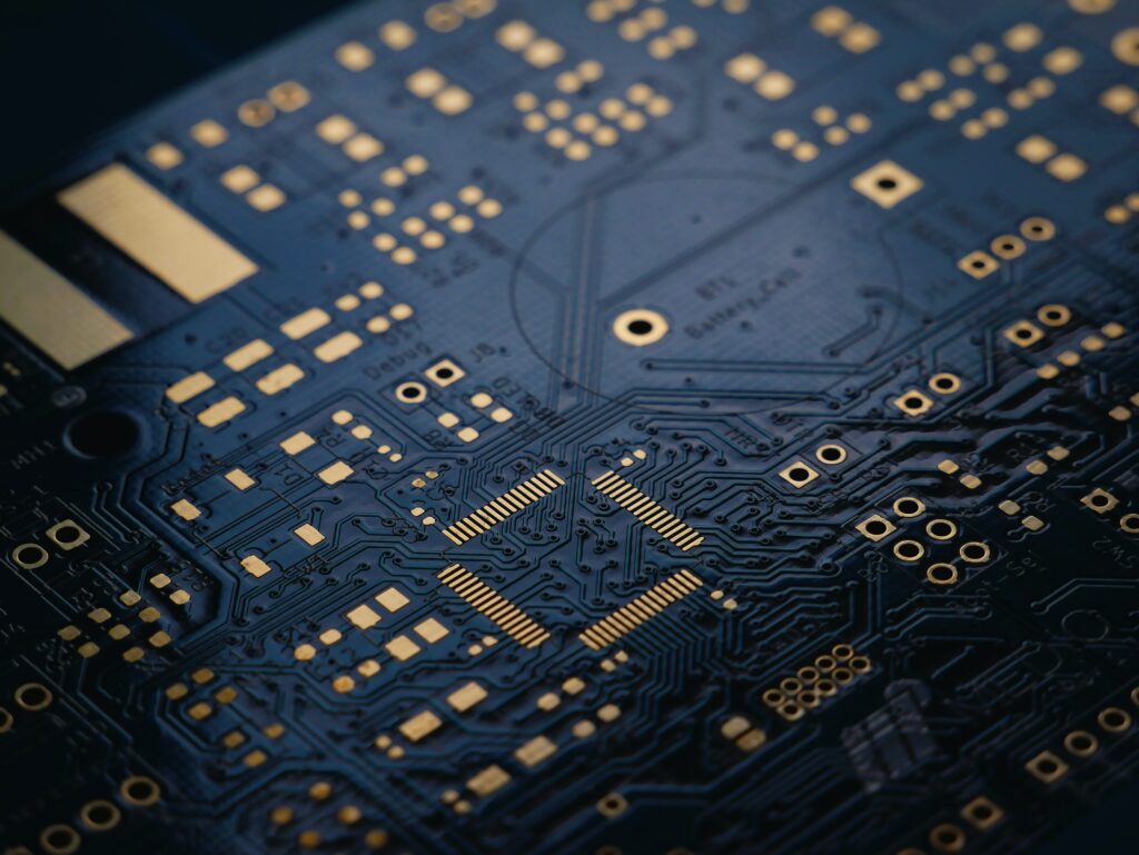
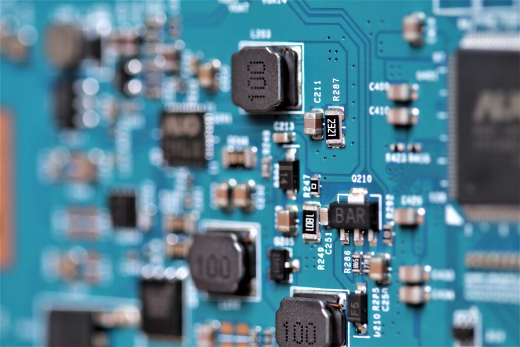
Our expertise lies in producing double-sided, multilayer, high-density, precision PCBs and PCB assemblies. Our company offers PCB Design services, fast delivery, large production, and samples to clients all over the world.
We provide customized printed circuit board design and layout for mixed-signal, Analog and digital boards. We can create printed circuit boards from scratch or enhance and optimize your current design for reasonably priced assembly. With highly-qualified and super experienced staff, we are well-positioned to provide good quality PCB design services.
Here are a few examples of the design capabilities that we offer.
- Analog and Mixed-Signal Designs
- High Density and Complex Designs
- High-Speed Digital Designs
- RF Designs
- Signal Integrity & EMI
- Compliance Engineering
WHY NEUROLAB?
1. Latest Technology
Our engineers are constantly focusing on the latest trends in electronic circuit design market and so have acquired the best practices and are known as experts.
2. On Time, On Budget & On Scope
We Always deliver finished products on time, on budget. Our in-house electronic design and production capabilities allow us to create the best results for our clients.All of our work has always been undertaken in close association with our clients, with confidentiality ensured.
3. Experienced Electronic Design Experts
To guarantee that we provide our clients with high-quality electrical design services, we refined and enhanced our procedures and products. We are such talented electronic designers because of this experience, which also enables us to provide you with such excellent service.
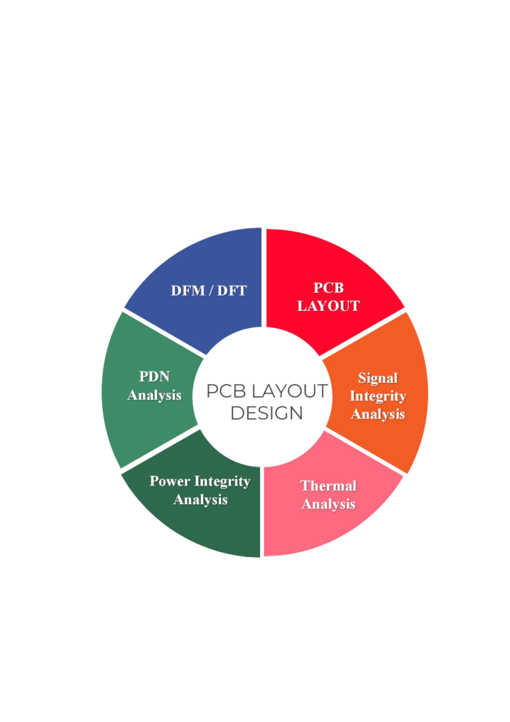
Design Capabilities
PCB Design of single-layer, multi-layer, rigid-flex PCB
- High-speed PCB design including differential pairs, length matching, etc.
- Highly Complex & Dense PCB layout designs.
- High speed, Multi-Layer, Rigid, Flex, Rigid-Flex PCB designs.
- In-Circuit Test data generation, Pick and place data generation, Drill, panel, and cutout drawings
- HDL, VIP, Back Drill, Blind and Buried vias
- Design for DFM/DFA
- Feasibility Analysis for Product Miniaturization
- Highspeed/High density/Highly Constrained Designs
- Controlled Impedance Design
- Low-level analog PCB designs.
- Ultra-low EMI designs
- Upgrade old PCB’s with outdated & obsolete components to the latest technology.
- Professional fabrication documents
- Advanced component footprints & library creation including BGA, QFN packages.